If you haven't already read our introduction to the new Raspberry Pi 3 B+, then go read it now before you read this detailed review of the Pi's new hardware! It'll give you a really nice overview of what's new.
And you can snag a new Raspberry Pi 3 B+ here!
In a nutshell, the new Pi 3 B+ has faster processing, faster wired networking,
and improved wireless networking that's now dual-band 802.11ac.
Warning! This article contains graphic images of a dissected Raspberry Pi 3 B+ that may disturb some readers!
Layout changes
Let's start by looking at a couple of our now-traditional diff images of the new Pi 3 B+ compared to the previous model, the Pi 3. In the images below, the parts in red are those that were different on the Pi 3.
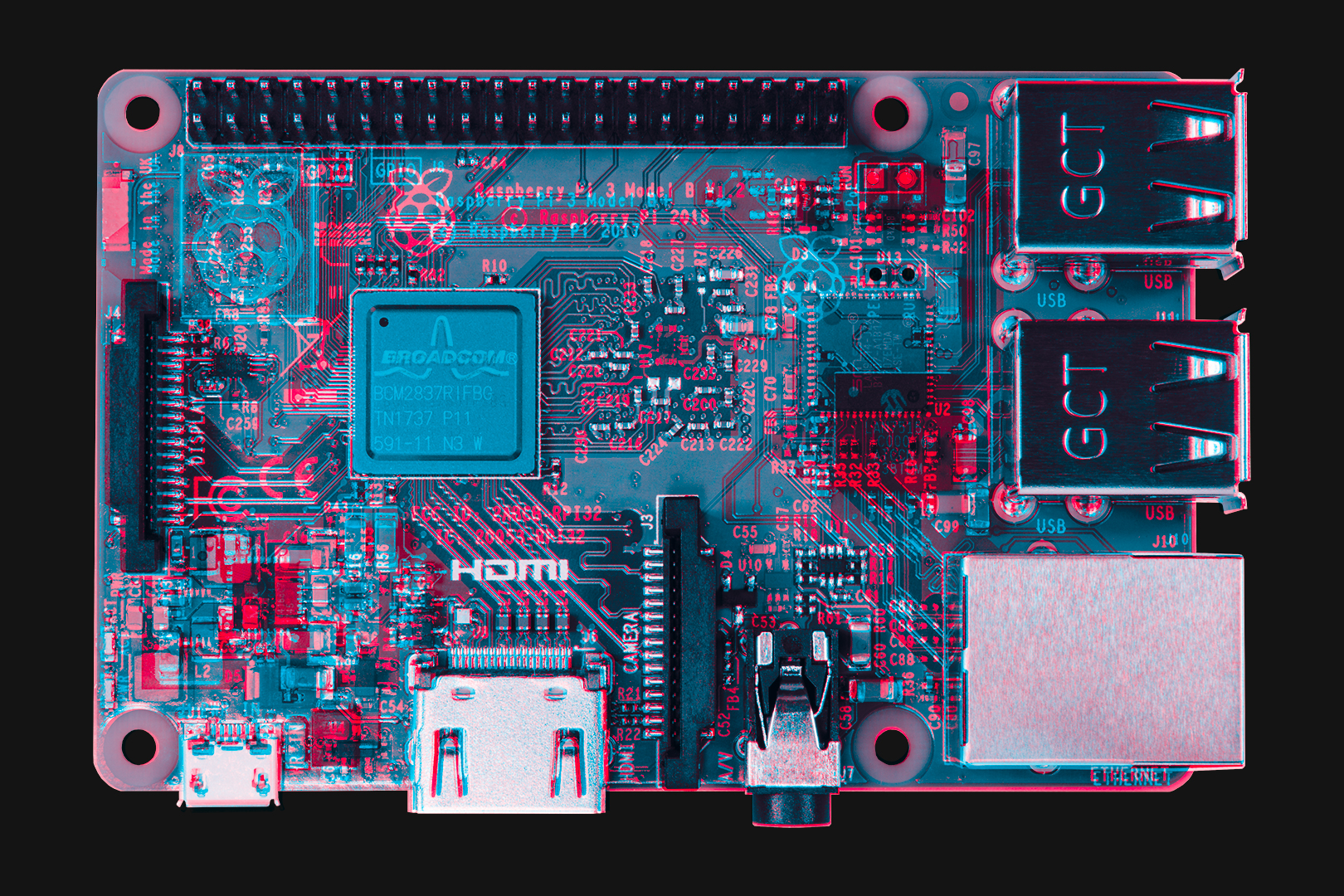
Looking at the top, you'll see that the redesigned 1.4GHz quad-core System on Chip (SoC) with metal shielding is in exactly the same location as the previous SoC on the Pi 3, although the traces running from it have moved around. More on the SoC later...
The next biggest change on the top side is the new wireless circuitry. All of the components have moved from the underside to the topside, and they're now hidden underneath metal shielding with the added touch of a Raspberry Pi logo embossed into the metal. The small, rectangular chip antenna at the top left on the Pi 3 is gone, and is replaced by the same PCB antenna, licensed from Proant AB, that's on the Pi Zero W.
Over on the right hand side, the LAN chip has shifted slightly and the four new Power over Ethernet (PoE) pins sit just below the GPIO. These will plug into the forthcoming PoE HAT from the Raspberry Pi Foundation and enable the Pi to get both power and networking over its pins through a single cable.

There are fewer changes on the underside. All of the major components - the RAM chip, and micro-SD card slot - stay in the same locations. The wireless circuitry is gone from the top right corner, since it had moved to the topside, as we mentioned. Some of the test points have moved around, and you'll notice that most of the part labels are gone (C1, C2, etc.)
System on Chip
The SoC is the same BCM2837 as on the Pi 3, but visually you'll see that it looks very different. The short story is that it has much better thermal performance, and so it can run at its full 1.4GHz quad core capability (on the Pi 3 it was under-clocked to 1.2GHz).
The previous SoC was in a plastic package, with bond-wires running inside, from the silicon die to the pins that connected to the Pi's PCB underneath. To fully understand how different the new one is, let's delve deep into the SoC itself.
Here's a (fake) x-ray image of the new SoC and the wireless circuitry; we'll talk about the latter later. Looking through the metal shielding of the SoC, you'll see a smaller rectangular object. That's the silicon die, that contains the CPU and GPU.

The die is soldered and bonded to a carrier PCB, that's the same square size as the metal shielding, and routes all of the pins from the die through to the underside where they're BGA-soldered to the Pi's PCB. BGA stands for Ball Grid Array, and it's a technique where the pins are arranged in an array on the underside of the chip, and small balls of solder on each pin are used to solder the chip to pads on the PCB.
We pried off the metal shielding from the top of the SoC, that was held on using a ring of adhesive round the outside with some thermal paste between the top of the die and the metal. This revealed the carrier PCB and die. We then desoldered the carrier PCB, revealing the BGA solder pads underneath.

Removing the die from the carrier PCB was really tough, as it was bonded as well as soldered, but a lot of heat and gentle prying got it loose eventually. The image below shows the carrier PCB after the die had been removed. You'll see that the top layer of the PCB actually came loose with the die, exposing the copper layer below. You'll also see all of the pins that connect the die to the PCB.

The die itself is pretty fascinating. Below, you can see part of it at full magnification on our inspection scope. The green is the top layer of PCB material stuck to it, but in the middle you can see the silicon of the die, and the grid-like structure of the features on the die. Each of those tiny vertical strips is just 10 microns wide (100th of a millimetre), and the small black square at the bottom (which may be a manufacturer's label?) is 0.1mm wide.

Performance-wise, the combination of the carrier PCB to route the pins through to the Pi, and the metal shielding to spread and dissipate the heat, means that the SoC is much more thermally-efficient and therefore can perform better and faster.
Wireless circuitry
There are several changes to wireless LAN on the Pi 3 B+ that combine to improve wireless performance. As we said, the circuitry is now all contained underneath metal shielding on the topside of the Pi, protecting it from interference both going into and out of the new PCB antenna.
The chip, that takes up most of the space underneath that metal shielding, is the Cypress CYW43455, with faster 802.11ac dual-band (2.4 and 5GHz) wireless LAN and Bluetooth 4.2. The Pi 3 used the Cypress CYW43438 chip, and 802.11n 2.4GHz wireless chip, as does the Pi Zero W.
Next to the wireless circuitry is the PCB antenna, which is visible as a translucent triangle. This antenna technology, licensed from Proant AB, is the same as is used on the Pi Zero W. It works by having a triangular cavity through the board's ground plane, within which radio waves can resonate and focus down to the narrow end of the cavity, where they are transmitted through to the rest of the wireless circuitry.

Ethernet
Ethernet on the Pi 3 B+ is gigabit ethernet over USB 2.0, meaning that speeds of 300Mbit/s are possible. This is significantly faster than the Pi 3's 100Mbit/s ethernet, although still not gigabit-capable.
The Pis 2 and 3 used the SMSC LAN9514 chip, a USB 2.0 and 10/100 ethernet chip, whereas the Pi 3 B+ uses a Microchip LAN7515 chip, theoretically capable of gigabit speeds, although limited by the speed of the USB 2.0 bus over which it runs to the SoC.
The rest of the Pi 3 B+'s hardware remains pretty much the same. There are some cosmetic changes to the positions of smaller components, test pads on the reverse, and the silkscreen on both sides of the board. Overall, the Pi 3 B+ will look and feel very similar to the Pi 3, that you're familiar with albeit with some very nice bumps to the speed of the processing, and to both wired and wireless networking.